Professional PCB Manufacturer

China PCB Manufacturer

Impedance Control PCBs

Impedance Control PCB

What is Impedance Control PCB

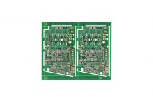
Impedance control PCB is a type of PCB that is designed to maintain a consistent impedance throughout the board. The impedance of a PCB refers to the measure of resistance to the flow of an alternating current (AC) signal. It is an important parameter that affects the performance of high-speed digital circuits and analog circuits.

As electronic circuits' operating speed has increased, so needs for PCBs to have controlled characteristic impedances, and the majority of PCB manufacturers are producing impedance control PCB for many applications.

Capabilities in Manufacturing Impedance Control PCBs

Victory PCB is a professional pcb manufacturer that can produce high-quality Impedance Control PCB products. Check our PCB manufacturing capabilities in the following table:
Monthy Capability3650 m²/month
Layer4 Layers
MaterialFR4, TG180
Finished board thickness1.6m
Min Trace Width/Space8/8mil
Min hole size0.25mm
Min copper in hole thickness1oz
Outer layer Finished copper thickness3oz
Inner layer base copper thickness3oz
Impedance Control Tolerance±10%

Why is Impedance Control PCB Necessary

When a signal needs a specific impedance to operate properly, controlled impedance should be preferred. In high frequency applications, keeping impedance constant on the complete electronic board is essential to protect the transferred data from damage and to maintain the clarity of the signal. The longer the trace or the higher the frequency, the more adaptation is needed. Any lack of rigour at this stage can increase the switching time for an electronic device or circuit and cause unexpected errors.

Uncontrolled impedance is difficult to analyse once the components are mounted on the circuit. Components have different tolerance capacities depending on their batch. Furthermore, their specifications are impacted by temperature variations which can lead to malfunctions. In such cases, replacing the component may seem to be the solution at first when, as a matter of fact, it is the unsuitable trace impedance that is the cause of the problem.

This is why trace impedances and their tolerances must be checked early on in the PCB design. Designers must work hand in hand with the manufacturer to guarantee the compliance of component values.

Factors That Affect Impedance Control

There are a few factors that affect the printed circuit board controlled impedance include: dielectric thickness, trace width, copper thickness, dielectric constant Er of the material selected for the stack, and thickness of the solder mask.

  • Trace width: The larger the trace width is, the lower the impedance will be. The thinner the trace width, the more impedance is offered. Increasing the board thickness increases the impedance while reducing it will decrease the impedance.

  • Dielectric thickness: dielectric thickness also affects impedance. The dielectric strength of a material is a measure of the electrical strength of an insulator. It is defined as the maximum voltage required to produce a dielectric breakdown through the material and is expressed in terms of Volts per unit thickness.

  • Copper thickness: The copper thickness is also considered while calculating the trace impedance in high speed and RF digital circuits.

  • Dielectric constant: The dielectric constant is the ratio of the electric permittivity of a material to the electric permittivity found in a vacuum. In a PCB, dielectric constant tends to vary inversely with frequency. A PCB with a low, stable dielectric constant is suitable for high frequencies and controlled impedance. A more difficult dielectric constant can often affect impedance in unpredictable ways.

Other Design Considerations

Trace lines should be kept as short as possible and reduce lengths wherever possible. If the trace lengths are fairly long, terminations should be used to prevent reflections.

Routing stubs and discontinuities, which add to the reflections and degradation of the signal quality, should be avoided.

For differential pair routing, try and ensure that the signal pairs have the same length.

Use of back drilling – for a thick backplane where the signal goes from the top layer to one of the inner layers, the remainder of the copper barrel of the via or the pin of the press-fit connector will be a stub, resulting in reflection. Back drilling removes the unwanted copper. It is a technique used to remove the unused portion, or stub, of the copper barrel from a thru-hole in a printed circuit board.

Consider using immersion silver as a surface finish rather than ENIG. Immersion silver results in less insertion loss (lossy) than ENIG purely because the nickel content in ENIG is very lossy and due to the skin effect, it is not very good for high-speed designs. The flatness of the pad is just as good as ENIG and it is more workable than ENIG.

Reduce the size of antipads on plane layers. Antipads are where pads are removed, or copper is removed on plane layers where the pad should not or does not connect to that plane. Sometimes the anti-pad size is too large creating unnecessary voids in the plane. By making the anti-pad a little bit smaller allows for more plane continuity resulting in a cleaner signal and return path.

How to calculate differential impedance

To ensure signal integrity in PCB designs with high-speed, there’s a need for great impedance characteristics in the connections of the conductor trace.

These can only be determined after the PCB’s controlled impedance is calculated based on the impedance specifications, layout, and layer buildup.

You can use impedance calculator online. It will help you calculate your trace widths, single-ended or differential impedances – for both microstrip and stripline models – and other parameters such as the dielectric height, the dielectric constant, and the trace thickness. The tool will also provide a guide for dielectric constant values for various PCB materials.

Also, you can contact us to get impedance calculation.

Impedance Control PCB FAQs

  • 1. What is Impedance?

    Impedance, measured in Ohms (symbol Ω), is somewhat different than resistance. Impedance is an AC characteristic, while resistance is a DC characteristic. Impedance becomes essential as the signal frequency increases, typically becoming critical for PCB traces at signal components of two or three hundred MHz and above.

  • 2. How does impedance control work?

    Impedance control involves specifying the required impedance for traces and transmission lines on your PCB. This is particularly important for higher speed signals and can be affected by your substrate material, copper widths, and routing.

  • 3. What are the 3 types of impedance?

    Impedance works with the help of three major elements, namely, inductor, capacitor, and resistor. It also gives an idea about the two types of impedance, i.e., the input impedance and the output impedance, and the types of resistance they provide.

  • 4. Why is impedance important in a circuit?

    Impedance—if not treated correctly—has a remarkably negative impact on circuit performance. Without the proper impedance matching, reflections can exist along the path from the source to the load.

  • 5. Why is higher impedance better?

    The higher-impedance has more winding in a coil which can result in a better motor system with fewer compromises resulting in the better overall sound & enhanced bass reproduction.

  • 6. Why is 50 ohm impedance used in PCB layout?

    50 Ohms is the least bad compromise between the impedance corresponding to minimum loss, maximum power, and maximum voltage.

  • 7. What is characteristic impedance in PCB?

    The most important of these is the characteristic impedance, which is simply the impedance of a transmission line on a PCB in total isolation from any other transmission line. This value is normally 50 Ohms, although it may take a different value depending on the signaling standard used in your device.

  • 8. What affects impedance in PCB?

    A few factors that affect impedance control during PCB design include trace width, copper thickness, dielectric thickness and dielectric constant.

Get custom impedance control printed circuit boards that authenticates your business products and makes it an element for quick turnaround at a first go! At VictoryPCB, we work with each customer to ensure they get the boards they need, the way they need them. Contact us today for a quote for your specifications.


×

Contact Us

×

Inquire

*Name
*Email
Company Name
Tel
*Message

By continuing to use the site you agree to our privacy policy Terms and Conditions.

Recruit global agents and distributors Join us

I agree