When we talk about PCBs, there a few different types of printed circuit board you might know. One of the most common PCBs is the 2 layer PCB. It has two layers of copper foil, which get separated by a dielectric material. In this post, we will show you everything about 2 layer PCBs that you need to know. Let’s dive right in!
2 Layer PCB, also known as double side PCB, is a printed circuit board with copper coated on both sides, top and bottom. There are circuit patterns on both sides and are connected through the via holes in the middle. Vias are small metal-plated holes on the PCB that can be connected to wires on both sides, so that the wires can be interleaved. That is, there are wirings on both sides, and components can be soldered on the front or the reverse. 2 Layer PCBs are also the most economical type of PCB to manufacture.

The double-sided circuit board solves the difficulty of staggered wiring in the single-sided board (it can be conducted to the other side through the hole), and it is more suitable for use in more complicated circuits than the single-sided board.
A 2 layer PCB can be anywhere from 0.010” to 0.060” thick. 2 layer PCB thickness standard thickness is 1.6mm. Our expectation is that the PCB fab has some copper clad cores, and the total thickness of copper and FR4 material is equal to 1.6mm.
In addition, the thickness of the board will depend on the dielectric material that you use and the size of the components mounted on the board. Also, the thicker the board, the better it is at reducing crosstalk between the signal traces.
The 2-layer PCB stackup contains 1 top layer and 1 bottom layer.
The 2-layer pcb has an inner layer which is also a copper layer. And this is where most of the vias get located. Plus, vias are the tiny little holes that connect the top and bottom layers together. More importantly, they allow for electrical signals to flow from one layer to another.
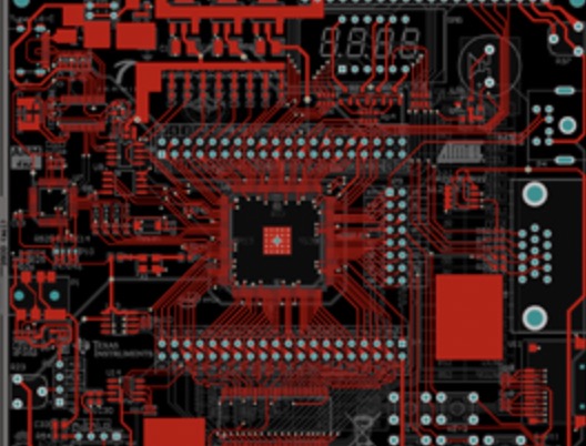
There are two signal layers on the double-layer board, which are Top Layer and Bottom Layer. The color of the Top Layer is red by default. You can see some pads and traces on it. In layman's terms, the red places are all copper. The place where the skin is, is where the solder can be attached and can conduct electricity.

The same as the bottom layer. The places with blue color can be tinned and conductive.
The power layer we use to distribute power to the different parts of the board. Also, you can use it as a return path for the ground signals.
The prepreg layer is a thin layer of dielectric material. And it can provide insulation between the copper layer. Besides, it can also provide support for the copper layers. The dielectric constant of the prepreg layer is 2. 2, which is lower than the FR-408 dielectric constant.
The solder mask layer is mainly used to place printing information, such as the outline and annotation of components, various annotation characters, etc.
Many 2-layer PCB design boards are created with limited performance. Usually, it is challenging to route a BGA package like a high-end microprocessor or FPGA in a 2-layer PCB board. It is not about the high PCB end boards, but several consumer microcontrollers, products, and IoT applications are created in a 2-layer PCB board. The good thing is that designing these boards is easy if you follow the below tips.
1. Employ 20 mil wide power traces, 6 mils wide signal trace, and 13 mils drilled diameter
Every designer wants to employ small features at no extra cost to achieve the routing of the highest density. You may perceive 6 mil wide signals trace to be too small; however, it holds 1A of DC current. It also possesses 80 milliohms/inch in something like 1 oz copper. For 20 mil wide power traces, it can use 3A of DC. It also possesses 25 mOhms/inch.
2. Power and signal paths on the first layer, route components, and ground return on the second layer
In case there is a progressive return path in the trace, it can be made longer without influencing the performance. The trick is employing the return path under one line. The simple method is utilizing a strong ground plane below the board.
3. Components adjustment for less crowded routing and have spaced signal traces
You can consider routing signals to minimize line-to-line crossing if you have the element placement. The traces possess high trait impedance and because they are situated far from the return plane, the crossing will be recorded. If the spaces are closer between the signal, then there will be a larger crossing.
4. Make a short route on the bottom layer. If it is challenging to keep the route short, include a return strap
The overall idea is coming up with an ideal design and offering a low impedance return path in all the signal lines. This is to ensure that the mutual inductance in the signal return path is maintained low.
5. Decoupling capacitors should be placed close to the IC power pin
Employ the huge size capacitor in a little body containing a voltage rating of up to 2x the required rail application. A capacitor of 22 uF MLCC is normally utilized. The capacitance amount relies on the draw of current on the elements you are decoupling. In case you don't research, consider 22 uF.
6. If possible, create one return for every digital signal on all the connectors
Switching noise or ground bounce is hugely contributed by several signals allocating similar return pins. In several connectors, one or two return pins can be used with several signal switching. This mostly applies to ground bounce.
Cost Savings: Double-sided PCBs are cheaper than 4-layer designs. This can save you money, especially if you're ordering a large quantity.
Easier Design and Production: Simple designs are faster to make, so you can get your PCBs sooner. They are also less likely to have expensive mistakes during the design or manufacturing process. If you need to fix your PCB later, double-sided boards are easier to repair than complex 4-layer PCBs.
Good for Large Orders: If you need a lot of PCBs, it's better to use 2-layer boards. They help with faster and cheaper manufacturing.
Quick Turnaround: Whether you have a big or small project, you might need a quick prototype. 2-layer PCBs are very fast to produce compared to other kinds of boards.
Simple Design: Double-sided PCBs have fewer fancy features. 4-layer PCBs can have more components and routing options, while 2-layer PCBs usually have a simpler design.
Slower Speed and Lower Capacity: If speed is important, more layers are better. Depending on your project, 2 layers may not be enough for the speed and capacity you need. Adding more layers, like going from 2 to 4, can give you more speed and capacity.
Bigger and Heavier: Even though they have fewer layers, double-sided PCBs can be bigger and bulkier to fit all the components and leads. If you have limited space, adding more layers is often a better choice to make the PCB fit in a small area.

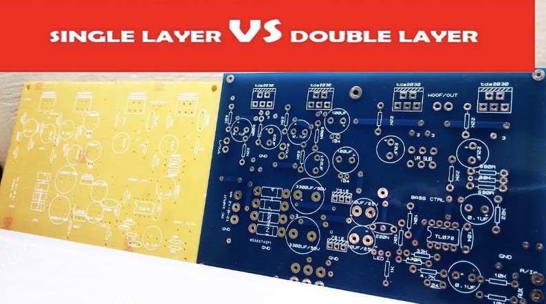
A single-sided board is the most basic PCB, where parts are concentrated on one side and wires are concentrated on the other side. Because the wires only appear on one side, we call this kind of PCB a single-sided (Single-sided). Because the single board has many strict restrictions on the design circuit (because there is only one side, the wiring cannot cross and must go around a separate path), so only early circuits used this type of board.
Single-sided PCB traces are present on only one side, while double-sided PCBs have traces on both sides with top and bottom layers. The components and conductive copper are mounted on both sides of a double-sided PCB, and this leads to the intersection or overlap of the trace. Double-sided PCBs are best for realizing high-density circuits that do not require point-to-point soldering.
| Single-Sided PCBs | Double-Sided PCBs |
| Conductive copper layer only on one side of the board | Conductive copper layer on both sides of the board |
| Suitable for basic circuit designs | Suitable for complex circuit designs |
| Mainly develops low-density circuit designs | Good for developing high-density circuit designs |
| Lower cost of manufacturing | Higher cost of manufacturing |
| Board manufacturing speed is high, producing a large volume of PCBs | Board manufacturing speed is slower, so the volume of production is lower |
| Lower cost of manufacturing | Higher cost of manufacturing |
| Occupies more space | Meets the space constraints in the circuit design |
| Less flexibility in circuit routing | More flexibility in circuit routing |
| There is no intersection or overlapping of traces | There is an intersection and overlap of traces |
| Easy to troubleshoot, debug, and repair | Difficult to troubleshoot and repair |
A 2 Layer PCB has two copper layers and A 4 Layer PCB features four layers of copper. The layers are laminated together with substrates. The top layer and the bottom one are the signal layers. But the inner ones are the ground and supply planes.
4 Layer Printed Circuit Boards are more powerful than single-layer PCBs and 2 Layer PCBs. But even though they are great for complex projects and remarkable for their functionality, their cost is higher than their 2-layer counterparts.
Price
A Two-Layer PCB is cheaper than a Four-Layer circuit board. However, the manufacturing cost is determined by the number of units you plan to order.
design and production
2 layer pcb has easier design and production and also it is easier to repair a double-sided PCB than to repair a Four-Layer PCB.
Lead Time
double-sided PCBs have an advantage over four layers and multilayer PCBs when it comes to lead time. Whether it is a small or large project, 2 Layer PCB takes a shorter lead time to make a prototype.
Durability
since the circuit board has many layers, it is more durable than a 2 Layer Printed Circuit board. Even though Four Layer PCBs are smaller than double-sided circuit boards, they are more substantial.
Applications
if your project is complex, the extra layers of 4 Layer PCB will be so beneficial. Since it is possible to be creative and add extra components, the PCBs can be used for complicated projects.
Size & Weight
4 Layer Printed Circuit boards are small and very light. They are smaller and lighter than double-sided PCBs because they need less room for wiring and components.
2-layer and 4-layer printed circuit boards offer different levels of functionality but are both beneficial for different types of projects. Ultimately, the choice between a 4 and 2-layer board primarily comes down to the specs of your project and the complexity of your circuit and the budget requirement you have for your project.
For more information about PCB fabrication and PCB assembly, contact VictoryPCB at 86-755-86339147 or contact us here.
How to Use Double-Sided Prototype PCB
The characteristics of double-sided PCB and the reasons for the complexity of the process