Multilayer printed circuit boards are made in six different ways. All of them differ significantly from each other in terms of the method, implementation and quality of the finished product. Further about each of them in more detail.
Multilayer PCB fabrication is a crucial type used in many instruments like computers, mobile, servers, televisions, power supplies, sensors, etc.
Firstly, it started in 1903. A German Inventor Alber Hanson made a PCB consisting of a flat foil conductor on an insulating board. There were multiple layers.
In the past, we dealt with regular boards. There were many limitations with those boards. Since 1903, the Electronics industry get revolutionized. The circuit of PCB is a more reliable, space saver, and Reproducible. It has many other features that will discuss in this article.
PCB fabrication has many types, such as
3. Rigid PCBs
5. Flex-rigid PCBs
7. High-Density Interconnect PCBs
8. In this article, we will discuss Multilayer PCBs in detail
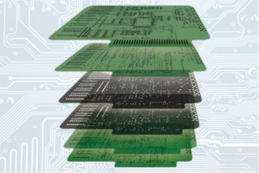
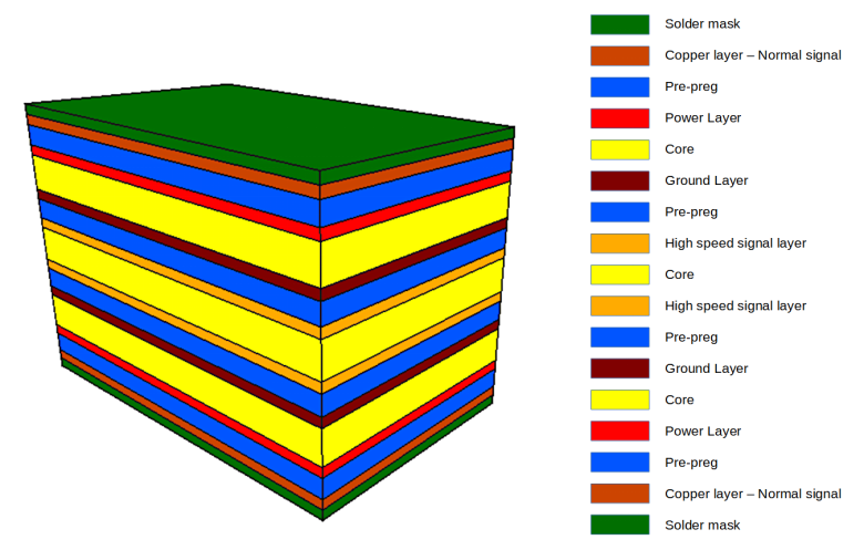
Multilayer PCBs have more than two conductive layers and insulating materials. These PCBs are used where we require complex circuits and high-density applications.

The multilayer fabrication process involves many steps.
1. Design
2. Material Selection
3. Drilling
4. Lamination
5. Etching
6. Plating
7. Finishing
Now we will discuss each step in detail:
Firstly draw a schematic diagram. It is a graphical representation of components and connections. This PCB design serves as a blueprint for the layout of the PCB.
Computer-aided design, or CAD, is used to create the format of PCB after that Gerber file is generated for the next step of the process.
After designing, we select specific materials which are necessary for the construction of multilayer PCBs. The choice of different materials depends upon the functionality and requirement of the specific application.

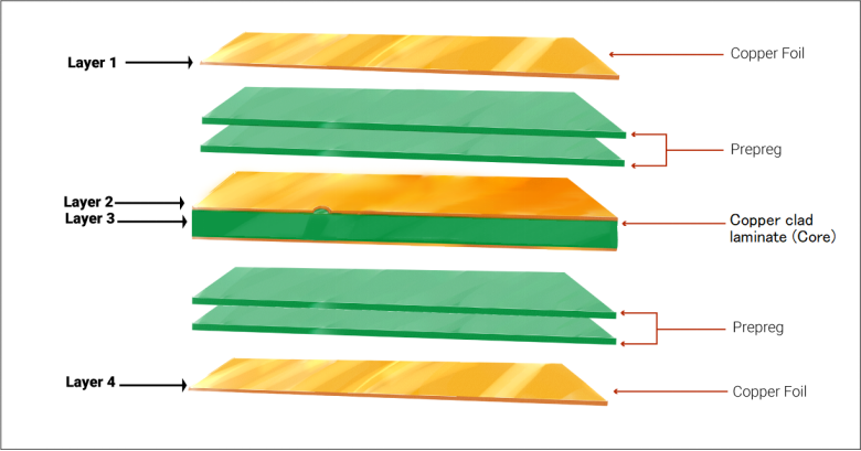
Generally, copper foil, insulation material, and adhesives are used in PCB. Additionally, there are many more materials, such as substrate materials, solder masks, silkscreens, stiffeners, and connectors.
A substrate is a material on which a circuit pattern is drawn. Fiberglass epoxy resins (FR-4) and polyimide (PI) are the best substrates. PI is used where PCB faces high temperatures, and FR-4 is used for general purposes.
Copper foil is used to tace conductive path on PCB. The thickness of copper foil depends upon the high-temperature application.
Solder mask comprises thermosetting epoxy material, used as a protective layer over copper traces. It is used to prevent copper tracing from corrosion and accidental short circuits.
Silkscreen is made up of black or white ink. It is used to label part numbers or text on PCB.
Adhesives bond different copper layers together.
Stiffeners are the main component of PCB which are used to strengthen the board at which any particular component is mounted.
Some connectors are also used to connect different components on PCB.
Drilling is a primary fabrication process. In this process, we create holes to place different components and connect between different layers of PCB.
We will discuss some basic steps of drilling.
Setup: Drilling is a sensitive step of the fabrication process. So, before drilling, set up the board and align it. Typically, CNC machines are used for drilling in PCB. All the information about the place and exact location of the hole is fed to CNC machines.
Drilling: PCBs are placed under the drill machine. It lowers on the board and rotates with high speed. It will cut the Substrate material and copper layer. By giving instructions to CNC Machines, we can increase the hole depth to the required result.
Cleanup: After the drilling process, cleaning or removing dust or debris is necessary. We use a vacuum or compressed air to clean up PCBs.
Final Cleanup: After the plating, a final cleanup removes any debris or remaining residue.
It is a crucial step in the processing of PCB fabrication. In this procedure, several layers of copper-clad are laminated and insulated to form a single PCB. We will discuss different steps of the lamination process.
To make the adhesion between different layers, prepare the different layers of PCB. Clean the copper surface.
Use epoxy resin on a copper surface. It is the best adhesive material applied in thin and even layers.
All the inner layers and insulating layers are stacked up. They are aligned so that all holes are for proper and precise cutting.
The whole stack of layers is placed into a lamination press. They are compressed and heated under high temperatures and pressure in that press. This process increases the strength of adhesive material so that all layers remain bound to each other.
Etching is a crucial step in the multilayer PCB fabrication process. This step removes residual copper from the board's surface to create the required circuits. Some specific steps are involved in the etching process:
The mask is thin, etch-resistant material used to protect the areas that are not to be etched. The mask is applied to the board's surface, where lamination is used.
UV light is exposed to the particular area of PCB after the masking. That particular part will become hardened, and the etching will resist.
After drilling, we use electroplating to connect different layers of PCB. In this method, a thin copper layer is deposited inside the hole.
The surface finish is the final coating on the PCB after assembling components. This surface finish protects copper traces from oxidation. A particular type of surface finishing is given as follows:
● HASL (Hot Air Solder Leveling),
● ENIG (Electroless Nickel Immersion Gold),
● OSP (Organic Solderability Preservative)
The essence of the method is the use of through holes. First, a pair of blanks is taken from a dielectric (usually foil). Then the following operations are carried out with them: Schematics of the inner layers are being made.
They are made by photochemical method. Further, special holes are created in the blanks, designed for interlayer transitions. Then the pressing operation is carried out.
At this time, the resin is finally squeezed out and fills the holes. After all the manipulations, the workpiece is processed in the same way as a standard board with two sides.
This production method has a key drawback - it can only produce boards whose number of layers does not exceed four. Sometimes this is not enough in terms of mounting density. However, the main advantage is relative simplicity.
The technology for the production of multilayer printed circuit boards with this option is based on the use of separate different layers. Moreover, only those that were obtained by etching can be used in production. The leads are connected through small perforated holes. This approach provides access of the upper layer to the lower ones.
The key disadvantage of the method is that it makes no sense to produce more than five layers. It has to do with print density. The fact is that the lower part has a lot of available space for tracing circuits, and the upper one has little.
This method of production does not have the previous drawback. It is carried out exclusively at the board manufacturer's factory. This is directly related to the emerging conclusions. The fact is that they come out of the inner layers into special perforated holes.
They need to be bent to the outside and made in such a shape that their geometry fits under the fastening block. So, the structure of the multilayer printed circuit board will not suffer. The main advantage of the method is simplicity and a small number of technological operations.
This has a positive effect on the cost of production. A similar advantage is relevant to the previous method. A key disadvantage is considered to be a lot of crosstalk.
Technically, this method of MPP production is no different from the version with pairwise pressing. The only difference is that the holes are not made through, but completely deaf. So, the outer layer is reliably protected from precipitation. But due to the use of blind holes, it is impossible to use foil in the manufacture. She breaks easily. The way out was the use of a special polyamide.