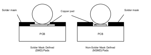
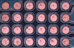
Generally, there are two kinds of pad designs: copper-defined pad and soldermask-defined pad. This article will briefly introduce the advantages and disadvantages of copper-defined pads and soldermask-defined pads.

The copper-defined pad is also called a non-soldermask-defined pad. The solder mask openings are larger than copper pads.

1) Good solderability: Because there are three sides of the pad, where tin can be applied.
2) It is also possible to precisely control the position and size of the pad.
3) It’s easier to design traces because the pad size is relatively small.
1) The copper foil is easier to be torn due to the external forces
2) Because the pad is small, the strength of the pad attached to the circuit board is relatively small.
Soldermask defined pad (SMD) is that the solder mask is coated on some copper foil and the copper foil which is not masked forms the pad. The soldermask openings are smaller than copper pads. Solder mask-defined pads are suitable for fine pitch components, often used with BGAs. The solder mask covers the pcb area between adjacent pads and overlaps on top of pad edges.

1) These pads will effectively improve the strength of the pads.
2) It improves the strength of BGA and reliability.
3) It’s a good choice for portal electronic products.
1) Worse solderability: The Solder Mask will be affected by the high temperature in the reflow oven, which will affect the tin area of the solder paste.
2) Worse position of the pads: The tolerance of soldermask is bigger than the copper, so it may affect the size of the pads and the relative position.
3) Because the copper area increases, the trace area is relatively reduced, and the trace design becomes more difficult.
4) The fabrication process is more difficult, and it requires high precision, greatly increasing the manufacturing cost
Victory is a professional PCB manufacturer established in 2005. Adhere to being a specialized manufacturer for multiple species, small to medium series, and quick turn production, we insist to provide 3H(high quality, high precision and high density) PCBs for our customers.
For more information about copper-defined pads and soldermask-defined pads, please do not hesitate to contact us.
By continuing to use the site you agree to our privacy policy Terms and Conditions.
Recruit global agents and distributors Join us