Our daily lives include a lot of electronics. Electronic components are found in everything, including our cars and smartphones. The printed circuit board, or PCB, is the brain of these electronics.
There are various steps in a PCB electronics assembly process. However, they must collaborate to create a seamless overall process.
The assembly of a PCB board will be covered in more detail in this article.

The various stages in the PCB assembly process include adding solder paste to the board, picking, and place of the components, soldering, inspection, and testing.
All these processes are required and need to be monitored to ensure that product of the highest quality is produced.
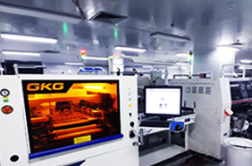
Solder paste must be applied to the sections of the board where solder is needed before the components are installed. The solder paste is a mixture of flux and tiny solder grains. This can be placed there using a technique that is very similar to various printing techniques.
A runner is pushed across the solder screen while squeezing a small amount of solder paste through the screen's holes and onto the board using the solder screen, which has been mounted directly onto the board and registered in the proper position. A board needs to have solder paste put to the regions where solder is needed before the components are installed.
Small solder grains combined with flux form the solder paste. This can be placed in position using a method that is quite similar to several printing methods.
A runner is dragged across the solder screen, which has been positioned on the board and is properly registered, squeezing a small quantity of solder paste through the screen's holes and onto the board.
The board with the additional solder paste is then sent into the pick and place procedure during this stage of the assembly process.
Here, components are picked up from reels or other dispensers by a machine that is stocked with reels of components, and they are then placed in the right spot on the board.
The stress of the solder paste secures the components that are adhered to the board. If the board is not jolted, this is enough to keep them in place. In some assembly procedures, tiny glue dots are added by the pick and place machines to affix the components to the board.
The printed circuit board design information is used to obtain the location and component information needed to train the pick and place machine. Because of this, pick-and-place programming can be greatly simplified.

The board is then put through the soldering machine as the following step in the assembly and production process after the components have been installed.
Even while some boards might be put via a wave soldering machine, this method is no longer frequently employed for surface mount components.
Solder paste should not be applied to the board when using wave soldering because the wave soldering machine provides the solder. Reflow soldering techniques are more frequently employed than wave soldering.
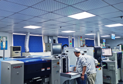
The boards are frequently examined after they have gone through the soldering process. Surface mount boards with 100 or more components or more cannot be manually inspected.
The automatic optical examination is a far more practical alternative. Some machines can inspect boards and find shoddy joints, misplaced components, and occasionally incorrect component.
Before they leave the plant, electronic products must be tested. They could be tested in a variety of ways. On this website's "Test and Measurement" section, you can get further perspectives on test methodologies.
Monitoring the outputs are required to make sure that the production process is functioning satisfactorily. This is accomplished by looking into any detected failures.
The optical inspection stage, which often comes just after the soldering stage, is the best location. This means that process flaws can be promptly found and fixed before a large number of boards are created with the same issue.
In this overview, the PCB assembly procedure for producing loaded printed circuit boards has been much simplified.
Contact us to purchase your PCB board and to discuss the services you need.
By continuing to use the site you agree to our privacy policy Terms and Conditions.
Recruit global agents and distributors Join us