In this series, I will explain the basic procedure for making a printed circuit board (PCB) using the free, open-source software (OSS) "KiCad."

This is the 3rd installment of the series, so we will input the circuit diagram and design the board layout.
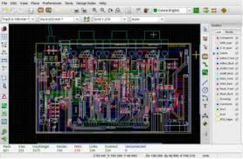
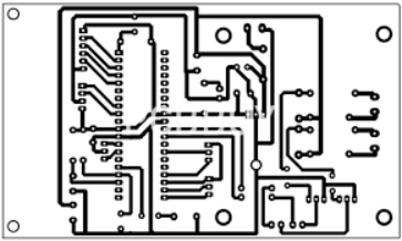
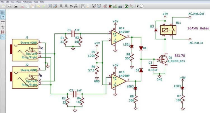
KiCad has a schematic editor called "Eeschema" and a circuit board layout editor called "Pcbnew." This time, we will use these powerful tools to design printed circuit boards and create "Gerber data" to be submitted to circuit board manufacturers.
Submitting this Gerber data to the board manufacturer is called "drawing." In this article, I will explain the specific procedure for printing.
The operating principle of this circuit is briefly explained below. It's not directly related to how to operate KiCad, so you can skip it. Still, if you understand the principle of how electronic circuits work, I think you'll have a lot more fun when making your own.
An astable multivibrator contains two transistors (bipolar transistors), "Q1" and "Q2". Since these transistors are turned on alternately, the LEDs "D1" and "D2" connected to their respective collectors alternately blink.
The period at which the LED flashes depends on the time constant of the resistor "R2" and capacitor "C1" connected to the base (B) of Q1 and the time constant of the resistor "R3" and capacitor "C2" connected to the base of Q2. It is determined by the time constant.
Click on the drawing area on the schematic editor to make it active, then press the [a] key on your keyboard. Wait for a while as the schematic symbol library is loaded. You can also click the "Place symbol" button on the left side of the screen without using the shortcut key.
Symbols for commonly used components such as "resistors," "capacitors," "inductors," "diodes," and "transistors" are all included in a library called "Device." A list of library names is displayed on the left side of this screen. The "Select Symbol" will be displayed when the schematic symbol library is loaded. If you are in trouble, we recommend first searching in the "Device" library.

The symbol "Q_NPN_EBC" just placed is explained briefly. In the KiCad library, symbolic names for transistors (both bipolar and MOS) begin with the letter "Q." The following "NPN" indicates the type of transistor.
This time, the transistor "2N5551" is an NPN-type bipolar transistor, so I chose a symbol that fits this. The footprint of the transistor prepared in KiCad is "1, 2, 3 in order from the left". The last "EBC" represents the actual pin arrangement. “EBC” stands for “Emitter (E) is Pin 1, Base (B) is Pin 2, and Collector (C) is Pin 3” . ).
Using other transistors, use the correct pinout when choosing the symbol. Also, if you use your own symbols or footprints, double-check that the pinouts are consistent.
The transistor "2N5551" used this time has a package called "TO-92" (shaped like a fish cake). Therefore, we will choose a footprint from the library "Package_TO_SOT_THT." This library contains many footprints for "TO" and "SOT" packages with leads (Through-Hole Technology). Select the footprint to associate with the symbol.
I chose the footprint "TO-92_Inline_Wide" from the "Package_TO_SOT_THT" library this time. This footprint has a pin spacing of 2.54 mm (100 mils), the same pitch as a typical universal board. Also, since the lead wires are arranged in a horizontal row (in-line), I think it will be as comfortable to use as when making a prototype with a universal board.
Double-click the footprint name to be used, and the footprint name will be registered in the "Footprint" column of the symbol property.
Also, the transistor model number "2N5551" is entered in the "Value" column. This is not essential for board design, but writing it to make the circuit diagram easier to understand is recommended.
After completing the above operations, click [OK] to return to the original circuit diagram screen. To close the property screen using the keyboard, press the [Shift] + [Enter] key (in place of the [OK] button) or the [Esc] key (in place of the [Cancel] button).
When inputting a circuit diagram, do not forget to register the footprint for each symbol. If you copy the "symbol after registering the footprint," like this time, the footprint information will be maintained even after the duplicated symbol. Using copy and paste in this way saves you the trouble of searching through the footprint library every time. However, please be aware that there is a possibility that you may mistakenly register a different footprint.
Press the [a] key to create the "Select Symbol" screen. Next, place the symbol for the LED (light emitting diode). This time we will use the symbol "LED_ALT" from the "Device" library.
After placing the symbol, move the mouse cursor over the symbol and press the [e] key to display the properties. Press the library reference button (bookmark) in the "Footprint" column to display the "Footprint Library Browser."

We selected the "LED_D5.0mm" footprint this time in the "LED_THT" library. This is the footprint for a 5.0 mm Diameter LED.
After selecting the footprint, enter the LED color "RED" to be used this time in the "Value" column of the symbol property screen and click [OK].
After that, duplicate one symbol and place it in an appropriate place in the same way as when placing the transistor symbol.
Next, place a symbol for a capacitor (electrolytic Capacitor). This time, I chose the symbol "CP" (Polarized Capacitor) in the "Device" library. Place this on the drawing.
"CP" stands for a footprint for polarized capacitors. "Radial" means that the two leads come out in the same direction. The word paired with this is "Axial," which refers to a shape in which lead wires come out from the left and right sides of the part. "D5.0mm" means "the diameter of the part is 5.0 mm".
The electrolytic Capacitor used this time is "100 uF, 16 V", and I chose this one because most capacitors with this capacity and withstand voltage have a diameter of about 5.0 mm.
The last "P2.50mm" means that "the lead wire pitch (Pitch) is 2.50 mm". 2.5 mm (100 mils) corresponds to one pitch of the universal board. If it is an electrolytic capacitor of about 100 uF, I think it can be installed at a pitch of 2.5 mm in most cases.
If you make a mistake in the pitch between pins, you cannot mount the parts on the printed circuit board, so please select the footprint carefully.
If you are using a part for the first time, we recommend that you check the dimensions in the datasheet. Also, when using general-purpose parts like this time, KiCad's standard library is sufficient. Still, when using special parts, it is faster to create a footprint yourself. In that case, please refer to the procedure explained in Part 2 of this series.
After selecting the footprint, enter the capacitor capacity "100u" to be used this time in the "Value" column of the symbol property screen and click [OK]. After that, duplicate one symbol the same way as before, press the [y] key to flip it horizontally, then place it in an appropriate place.
Next, place the resistor symbol. The resistor symbol uses "R" from the "Device" library. (I am familiar with the jagged symbols of the old JIS, so I usually design using my own jagged resistor symbols.)
Prepare "pads" for soldering the lead wires of the battery box. In such cases, it is convenient to use the "TestPoint" symbol from the "Connector."
"THTPad" refers to a pad with a hole for inserting lead wires. On the other hand, the one named "Pad" is just a pad with no holes and just an exposed copper foil. "D2.0mm" means that the overall Diameter is 2.0 mm.
"Drill1.0mm" means the hole diameter (drill diameter) is 1.0 mm. When using general electronic parts, lead wires, tin-plated wires, etc., a hole with a diameter of 1.0 mm can handle most of them.
By continuing to use the site you agree to our privacy policy Terms and Conditions.
Recruit global agents and distributors Join us