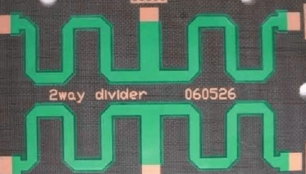
Impedance matching is a crucial concept in electronics and PCB design. As a PCB engineer, understanding impedance matching is essential for ensuring optimal signal integrity and efficient power transfer in electronic circuits.
Impedance matching refers to the practice of adjusting the impedance of a component or transmission line to match the impedance of the source or load it's connected to. Impedance is the measure of the opposition to the flow of alternating current (AC) in a circuit, and it consists of both resistance (R) and reactance (X), which can be inductive or capacitive.

In PCB design and high-frequency circuits, impedance mismatches can lead to several issues, including:
Reflections: When there's an impedance mismatch between components or transmission lines, some of the signal energy may be reflected back to the source, causing signal distortion, loss, and possibly interference with other parts of the circuit.
Signal Integrity: Impedance mismatches can result in signal degradation, leading to ringing, overshoot, undershoot, and reduced data transmission quality, especially in high-speed digital circuits.
Power Transfer: In RF (radio frequency) and microwave circuits, impedance matching is essential for maximum power transfer between components and to prevent power losses.
Efficiency: In power amplifiers and other circuits, impedance matching ensures that the maximum power is delivered to the load, optimizing the overall efficiency of the system.
Impedance matching is a critical aspect of PCB design that ensures optimal signal integrity and performance. Following these key steps and considerations for achieving well-controlled impedance on a printed circuit board. Whether you're working with microstrip traces, striplines, or other high-frequency designs, understanding these principles is essential.
Well-controlled impedance means that the trace impedance remains constant along the entire path on the PCB. Regardless of changes in layers or routing, the impedance should be uniform from the source to the destination. While we don't have direct control over impedance in the driver or load, we can regulate it on the PCB through matching circuitry. This consistency ensures a reliable signal path.
The choice of materials plays a vital role in impedance control. For high-speed designs, traditional materials like FR4 may no longer suffice. Opt for laminates with a lower dielectric constant (Dk) to enhance signal performance and minimize signal distortion, especially for frequencies of 1 GHz or higher. Materials like Isola FR408 with a consistent Dk of 3.7 are ideal for maintaining impedance consistency. Ensure compliance with IPC4101 grade for the bare laminate used in the PCB fabrication process.
Consider the loss tangent or dissipation factor, a measure of signal loss as it propagates down the transmission line on the PCB. For high-frequency designs, select materials with the lowest loss tangent to minimize signal degradation. Different laminates exhibit varying loss tangents, making the right material selection crucial.
Maintaining good dielectric spacing between the copper and the laminate is essential for consistent electrical performance of traces across the PCB. Additionally, pay attention to the fiberglass weave pattern used in constructing the PCB core and prepreg substrates. A tighter weave pattern ensures a more uniform dielectric constant, enhancing impedance consistency and minimizing trace impedance variation and propagation skews.
For controlled impedance, microstrip and stripline transmission lines are commonly used. The characteristic impedance of these traces depends on factors like the dielectric constant, thickness of the insulating material, as well as the width and thickness of the trace. Choose appropriate values based on the operating frequency of the circuit, ensuring that the impedance remains within the desired range.
Explicitly indicate which signals require impedance control, using component datasheets as a fundamental reference. Pay close attention to clock or data lines of DDR memories, audio/video signals, gigabit Ethernet, and radio frequency (RF) signals. Indicating the appropriate layer for routing and spacing rules between traces is crucial to maintain expected impedance values.
Appropriately space traces with controlled impedance, following rules such as the "2W" or "3W" spacing for microstrip transmission lines. This spacing minimizes crosstalk. Adjust spacing based on the signal frequency, increasing it for high-frequency signals to achieve better isolation.
Limit the use of vias and bypass capacitors between pairs of differential signals. Placing components and vias symmetrically around these signals reduces impedance discontinuities, ensuring signal integrity.
Balancing trace lengths is crucial to prevent propagation delays, especially for high-speed signals. Techniques like adding serpentines to shorter tracks can compensate for length differences, minimizing impedance discontinuities and ensuring simultaneous signal arrival.
A comprehensive approach to impedance matching leads to enhanced signal quality, reduced reflections, and reliable performance in high-frequency applications. This process is essential for modern PCB designs, particularly in advanced technologies where impedance control is critical for optimal functionality. Contact us to learn more about impedance matching today!
By continuing to use the site you agree to our privacy policy Terms and Conditions.
Recruit global agents and distributors Join us