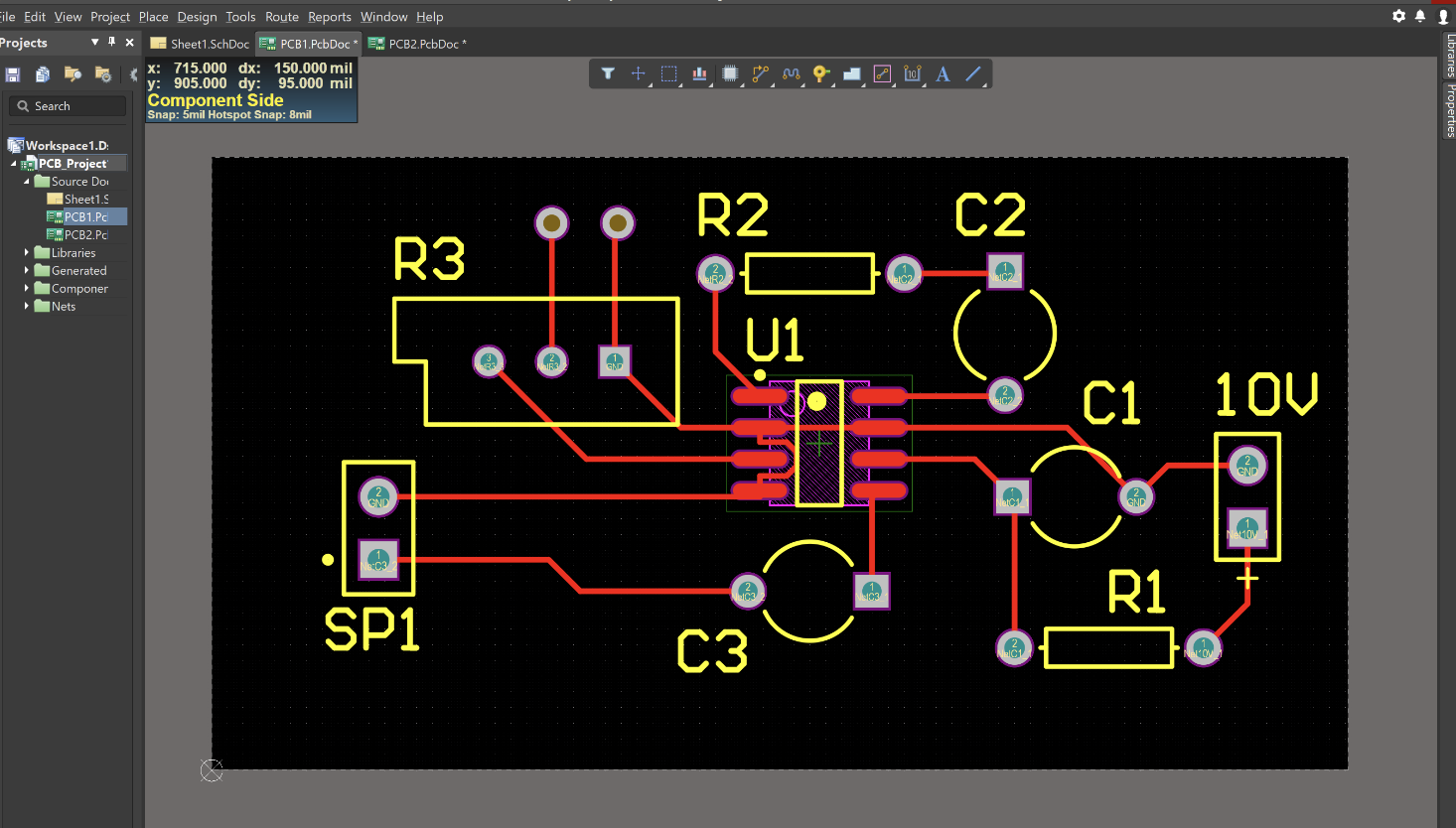
The evolution of Gerber files marks a pivotal shift in the landscape of pcb production. Prior to their adoption, the absence of a standardized guideline led to a maze of diversified content formats — from graphic to textual, bitmap to vector — each with its own set of challenges. Incompatibilities in measurements, dimensions, and positioning often fostered confusion and misunderstandings between customers and production companies. However, with the embrace of the Gerber format, a new era of universal compatibility dawned, enabling seamless collaboration between PCB designers and manufacturers. Now, armed with a file format independent of CAE/CAD software, manufacturers navigate production with newfound clarity and precision, streamlining processes and ensuring seamless communication throughout the PCB production journey.
A PCB Gerber file is a standard file format used in the electronics industry to convey the design information necessary for the fabrication of printed circuit boards. Developed by Gerber Scientific, the Gerber file format consists of a set of ASCII text files, each representing a different layer of the PCB design. These layers typically include:
Top Copper Layer: Contains the traces and pads on the top side of the PCB.
Bottom Copper Layer: Contains the traces and pads on the bottom side of the PCB.
Solder Mask Layers: These layers define where solder mask should be applied to protect copper traces during soldering.
Silkscreen Layers: These layers define where component designators, logos, and other markings should be applied.
Drill File: This file specifies the locations and sizes of all holes to be drilled into the PCB.
Rather than a single document, the format encompasses a collection of files, collectively defining the blueprint for PCB production. These files detail electrical connections, tracks, vias, and pads, presenting vector-based instructions in the form of graphic objects. Moreover, they provide precise guidelines for hole placements on the PCB, ensuring accurate reproduction of the intended design during manufacturing.

(source:altium)
Today, PCB manufacturers solely require this documentation from customers. Major electronic design software offer the capability to export designs in this format, making it essential for electronic designers to verify its availability in their CAE software. RS-274X, the current standard format, consolidates configuration parameters, openings, XY coordinates, draw, and flash commands within a single document, providing a powerful and comprehensive solution for PCB fabrication.

Gerber File Formats refer to the various standards and versions of Gerber files used in the PCB manufacturing industry. Over time, Gerber file formats have evolved to accommodate advancements in technology and the growing complexity of PCB designs. Some common Gerber file formats include:
RS-274-D, an early Gerber file format, standardized PCB design data for fabrication. ASCII text files represent PCB layers, detailing elements like copper traces and holes. While widely used for simpler designs, it lacks features of newer formats like aperture definitions. Transition to newer formats, such as RS-274-X or Gerber X2, offers enhanced capabilities for complex designs.
RS-274-X, also known as Extended Gerber, is an advanced Gerber file format used in PCB manufacturing. It builds upon RS-274-D, introducing features like aperture definitions and embedded apertures. This allows for more precise representation of PCB designs, especially for complex layouts. RS-274-X files are ASCII text documents that describe the shapes, sizes, and positions of elements on each layer of the PCB. They offer enhanced compatibility with modern CAD/CAM software and are widely used in the industry for creating high-quality PCBs.
Gerber X2 is an extension of the RS-274-X Gerber file format, introducing enhancements for better communication of design intent in PCB manufacturing. It includes additional information such as stackup data, component placement, and netlist information. Gerber X2 aims to improve collaboration between PCB designers and manufacturers by providing a more comprehensive set of data, facilitating smoother production processes and ensuring greater accuracy in PCB fabrication.
ODB++ is a comprehensive PCB manufacturing format that extends beyond Gerber files. It includes not only the Gerber data but also additional information such as component placement, netlists, design rules, and manufacturing instructions. ODB++ aims to streamline the PCB manufacturing process by providing a single, unified format for all necessary data, improving communication between designers and manufacturers, and reducing the potential for errors during production.
IPC-2581 is a comprehensive PCB manufacturing format developed by the Institute for Interconnecting and Packaging Electronic Circuits (IPC). It aims to standardize the exchange of PCB design and manufacturing data between designers, manufacturers, and assembly houses. IPC-2581 encompasses not only Gerber data but also additional information such as component placement, netlists, design rules, stackup information, and assembly instructions. By providing a unified format for all necessary data, IPC-2581 streamlines the PCB manufacturing process, improves communication, reduces errors, and enhances overall efficiency in the industry.
One of the popular CAD systems includes a handy SAP engine that allows you to upload an SAP file and quickly generate files for your project.
In our example, we'll upload a Gerber RS-274X SAP file, and from that, we'll get five separate Gerber files for the LED Flasher project we completed in the PCB Design Basics series.
Open the PCB design (.brd) File in the CAD control panel;
Select the CAM Processor tool at the top of the window, or select File>> CAM Processor to open the CAM Processor Dialog;
No SAP task has been loaded yet, so let's add one. Select File >> Open >> Job (File >> Open >> Task). Then navigate to the default project folder, and select the gerb274x. Cam file and click Open.
As you can see, new tabs for each SAP file will now be generated as a result of this task. Click the Process Job button to create all Gerber files.
And that's it! With the click of a button, you generate all the Gerber files you need, which you can then send to the PCB manufacturer. If you return to the CAD control panel, you will see the newly created Gerber files listed next to the existing project files.
Hole File Formation
Since the Gerber files you just generated contain all the necessary information a manufacturer needs to produce each PCB layer, they do not contain information about the holes to be drilled. You need a file that lists the location and size of each hole.
Fortunately, generating such a file in modern CAD is as simple as creating Gerber files.
Select the CAM Processor tool at the top of the window, or select File>> CAM Processor to open the CAM Processor Dialog.
First, you need to download the SAP task for drilling holes. Select File >> Open >> Job (File >> Open >> Task). Then navigate to the default project folder, and select the excellent. Cam file and click Open.
Now there will be only one tab, Generate drill data (Generate data about the holes), in which the data from the layers 44 Drills (44 Holes with plated) and 45 Holes (45 Holes without plated) will be summarized - exactly what you need. Click the Process Job button to create this File.
CAM engineering software is indispensable in the creation of printed circuit board designs, leveraging manufacturing data extracted from Gerber files to generate intricate two-dimensional or three-dimensional representations. These software systems serve as the backbone of PCB fabrication, orchestrating crucial processes such as etching copper layers, creating component pads and connection traces, drilling required holes, and profiling the board to precise specifications. Gerber files act as the primary conduit for transmitting design information to CAM systems, providing comprehensive instructions necessary for every stage of PCB production.
Upon importing Gerber data into CAM systems, files are meticulously organized and labeled, ensuring alignment and archival in their original format. Engineers then undertake crucial manipulation tasks to refine the designs for production-ready layouts, whether in singles or within an array configuration. Clean-up processes play a pivotal role in ensuring error-free production, with engineers conducting both manual and automated clean-up procedures on each layer of the PCB design. Throughout these meticulous tasks, design rule checks are meticulously calibrated to parameters tailored to the specific type of PCB being assessed, safeguarding against potential manufacturing discrepancies.
Engineers rely on guidelines and references embedded within the Gerber files as they manipulate the data within CAM software. These files serve as comprehensive guides throughout the product development lifecycle, elaborating on requirements at each stage of PCB fabrication and assembly. With their seamless integration into CAM engineering software, Gerber files not only streamline the PCB design process but also serve as indispensable tools for ensuring precision, accuracy, and adherence to design specifications in both fabrication and assembly processes.
Ready to elevate your PCB projects to new heights? Explore our comprehensive guide on PCB Gerber files to unlock the full potential of your designs. Then, trust VictoryPCB, your professional PCB supplier, to bring your visions to life. With our expertise and commitment to excellence, we're your partner in success. Contact VictoryPCB today via sales@victorypcb.com to discuss your PCB needs and let's turn your ideas into reality!
By continuing to use the site you agree to our privacy policy Terms and Conditions.
Recruit global agents and distributors Join us