Having a basic understanding of printed circuit board terminology can make working with a PCB manufacturing company much faster and easier. This glossary of circuit board terms will help you understand some of the most common words in the industry. While this isn't an all-inclusive list, it is an excellent resource for your reference.
Annular Ring — A copper ring on a metallized hole on PCB.
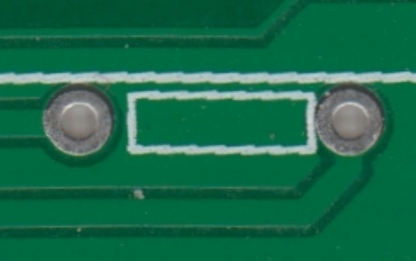
DRC — A procedure to check the design for errors, such as shorted traces, thin traces or small drilled holes.
(Gold) Finger — The exposed metal pad on the edge of the board is generally used to connect two pcbs.
Stamp Hole — Another optional way to split board. With some continuous holes to form a weak connection, the board can be easily split.
Pad — An exposed portion of metal on the surface used to solder.
Panelization — A large circuit board made up of many small, divisible circuit boards. Automated circuit board production equipment often has problems when producing small boards. Combining several small boards together can speed up production.
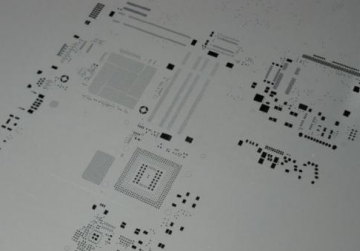
Stencil — A thin metal stencil (or plastic) that is placed on the PCB to allow the solder to penetrate through certain areas during assembly.
Plane — A continuous section of copper on a circuit board. It is generally defined by boundaries, not paths, also known as "copper pours".
Metallized Via — A hole in a PCB that contains an annular ring and plated hole walls. A metallized via may be a connector connection point, a signal transition or a mounting hole.
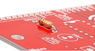
Reflow Soldering — Melts the solder to connect the pads and device pins together.
Silkscreen — Letters, numbers, symbols or graphics on the PCB board.
Slotted — Refers to any hole in the PCB that is not round. Slots may or may not be plated.
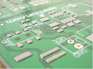
Solder Paste Layer — Before placing components on the PCB, a certain thickness of solder paste layer will be formed on the pads of the surface mount devices through the stencil. During the reflow process, the solder paste melts, creating a reliable electrical and mechanical connection between the pads and the device pins.
Soldering Oven — An oven for soldering plug-ins. Generally, there is a small amount of molten solder in it, and the board can pass through it quickly, and the exposed pins can be soldered.
Solder Mask — To prevent short circuits, corrosion and other problems, copper is covered with a protective film. The protective film is generally green, but other colors are possible.
Soldering Tin — Two connected pins on a device are mistakenly connected together by a small drop of solder.
Surface-mount technology — An assembly method in which the device simply needs to be placed on the board without passing the device pins through the vias on the board.
Thermal Pad — Refers to a short trace that connects the pad to the plane. If the pads are not properly thermally designed, it is difficult to heat the pads to a sufficient soldering temperature during soldering.
Trace — On a circuit board, a generally continuous path of copper.
V-cut — Make an incomplete cut on the board and the board can be broken through this straight line.
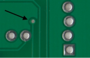
Via — A hole in a board, typically used to switch signals from one layer to another. Plug hole refers to covering the solder mask on the via hole to prevent it from being soldered. Connector or device pin vias are generally not plugged because they need to be soldered.
Wave Soldering — A method of soldering plug-in devices. Passing the board at a constant speed through a molten solder furnace that produces a steady wave of solder that solders the device pins and exposed pads together.
Victory is a professional PCB manufacturer which established in 2005. Adhere to be a specialized manufacturer for multiply species, small to medium series, and quick turn production, we insist to provide 3H(high quality, high precision and high density) PCBs for our customers. If you have any inquiry, please do not hesitate to contact us.
By continuing to use the site you agree to our privacy policy Terms and Conditions.
Recruit global agents and distributors Join us