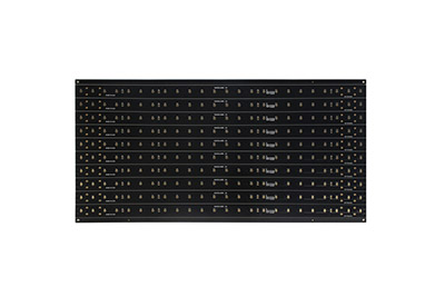
Heavy copper printed circuit boards are specially designed wiring systems where the inside and outside layers are made with 3 oz of copper or more.
Those with 4 oz of the metal are also included. One important feature which is carefully monitored during its design is the thickness of the metal since it affects the durability of the circuit board.
To guarantee reliable PCBs, the correct thickness proportion alongside selected high-quality material with compact plating is very critical in its design. Hence, there is a need for you to partner with a trusted and reliable heavy copper PCBs manufacturer with many years of experience in the industry.
PCBs which are compact have become increasingly popular in the PCB industry as they are being used in a great number of electronic gadgets as a result of their immense benefits.
Since electronic gadgets are in most cases used in a demanding area which need to resist heat stress, hence the incorporation of heavy copper PCBs into the various electrical circuit. With this in place, the possibility of failure is reduced to the barest minimum as they help to conduct heat away.
Hence, these printed circuit boards are in huge demand, although they are high-priced.
Trace width-a significant factor
One of the yardsticks for evaluating the competence of a PCB manufacturer is based on the trace width of the circuit board produced. It is one of the most significant factors that should be consistently checked when modeling PCBs as it has influenced the size and layout of the circuit board.
Following the specifications, experienced PCBs manufacturers ensure that the right trace width has enough space
However, the trace width is a function of the metal weight i.e. the thickness of the metal is directly proportional to the trace width.

By interpretation, it means that the higher the thickness, the more space it requires, and the lower the thickness, the less space is needed. Using the correct trace width is very cardinal to the proper functioning of the PCBs.
The recent specification indicates that 0.5 oz requires 0.003 trace width, 2 oz metal requires 0.008 and for a 4 oz metal, 0.016 trace width is needed.
The advantages
The following benefits make heavy copper PCBs suitable for electronic products and the electrical industry.
1. Enhanced current conductivity
2. Minimizes the size of PCBs
3. Increased strength of the connector site
4. It helps in the incorporation of metals of multiple weight on the same circuit layer
5. Complexity in wire buss design is eliminated
Applications
Printed circuit boards that are thick are used for different purposes high power relay, heat dissipation, power converters, and many more.
Several industries are in great demand for these products such as the automobile, communication, medical, industrial control, and the military.
In addition, they are also very relevant in the storage pumping system, rail traction system, protection, and signal relay system.
In equipment where there is a release of a large amount of heat such as the welding machine, they helps in conducting the heat away fast so as to ensure optimum functioning and performance of the equipment.
In Need of a high-quality heavy copper PCB?
Heavy copper PCBs are very essential in the manufacture of electronic products as they help in channeling the heat away and enhance their overall performance and durability. Its skyrocketing demands imply that there will be numerous products of its kind in the market with higher chances of compromise in quality.
Here at ShenZhen Victory Electronic Technology Co., Ltd. We have well trained and skilled professionals and high-quality materials at our disposal to build a first-class grade heavy copper PCB. Kindly give us a call and make your order today! A trial will give you a million reasons to come back.
By continuing to use the site you agree to our privacy policy Terms and Conditions.
Recruit global agents and distributors Join us