Professional PCB Manufacturer

China PCB Manufacturer

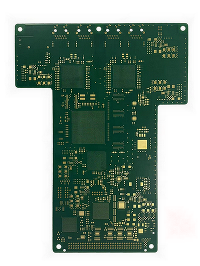
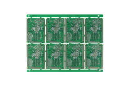
14L High Density HDI Immersion Gold PCB with 1.5oz Finished Copper Thickness 14L High Density HDI Immersion Gold PCB with 1.5oz Finished Copper Thickness

Quantity:
Share this:

Product Description

14L High Density HDI Immersion Gold PCB for Telecom Device


Victory able to provide High Density PCB Prototypes, small and medium-volume High Density PCB.

We not only produce High Density PCB Prototypes, small and medium-volume High Density PCB is also no problem. We can make up to 48 Multilayer PCB, Min. Hole Size 4mil, Min. line width/space 3mil.


Find out about our more info, Please contact us at sales@victorypcb.com.


Monthy Capability: 3900 Sq M/Month

Layer: 14 Layers

Material: FR4 TG180

Finished board thickness: 2.0mm

Outer layer Finished copper thickness: 1.5oz

Inner layer base copper thickness: 1oz

Min Trace Width/Space: 3/3mil

Min hole size: 0.2mm

Min hole wall copper: ≥25UM

Soldermask Color: Gloss Green

Silkscreen Color: White

Surface finishing: Immersion Gold 

Application field: Industrial control


Advantage of Victory PCB

  • A Professional PCB Manufacturer since 2005

  • Small and Middle/Large batches, Multiple Varities, Short Lead Time

  • Certificated with UL (E315391), ISO 14001, IATF16949, ISO 9001, SGS, ISO13485, SA8000

  • Capablity 60,000Sqm/3000PNs per month, 500staffs

  • Make oversized board (reach to 1200mm)

  • Quotation will be provided within 12hours

  • 15 years experience on PCB exporting

  • 10% sales revenue invested in R&D and advanced automatic equipment from Japan, Taiwan and Germany every year

  • Product:Single Sided, Double Sided and Multilayer PCB, Rigid PCB,Flex PCB,Rigid-flex PCB,AL-base PCB.

PCB Production Capability

Material CEM-3,FR-4(Normal to High Tg),High CTI FR-4,PolyImide(PI) ,Aluminum Base,Rogers
Surface finish HAL, HASL Leadfree, ENIG, Chem Tin, OSP, Gold Finger, Immersion Silver, ENEPIG
Min. Core thickness 4mil/0.1mm
Prepreg type 1080, 2116, 7628, 106, 3313, 2165, 1500.
Max board size 24.41X47.24inch/620X1200mm
Copper thickness Min. base copper 1/3Oz
Max. base copper 10Oz
Min. board thickness 2- Layer 0.2mm/8mil
4-Layer 0.35mm/14mil
6-layer 0.65mm/26mil
8-Layer 1.0mm/40mil
10-Layer 1.3mm/51mil
12-Layer 1.6mm/63mil
14-Layer 1.8mm/71mil
16-Layer 2.0mm/79mil
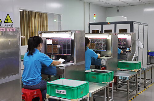
AOI (Automatic Optical Inspection) Max.table size: 685X685mm
Max.inspect size: 620X620mm
Max. thickness: 3.20mm(126mil)
Min. thickness: 0.10mm(4mil)-core
Min. width/gap: 3mil/3mil
Board thickness Tolerance ±0.10mm(4/6layers)
±0.13mm(8/10layers)
±0.15mm(12/14/16layers)
Max.board thickness 6.0mm/236mil
Min.line width/space 3/3mil
Min hole size 4mil/0.1mm
PTH wall thickness ≧25µm
Max. aspect ratio 12:01
PTH dia. Tolerance ±0.075mm/3mil(Standard), ±0.05mm/2mil(Advanced)
NPTH dia. Tolerance ±0.05mm/2mil(On laminate area)
±0.03mm(On ground area)
Hole location Tolerance ±0.075(Standard) ±0.05mm(Advanced)
±0.13(2nd drilled hole to 1st drilled hole location (mm)
Slot size tolerance ±0.075mm(board thickness≤1.0mm)
±0.10mm (board thickness>1.00mm)
V-CUT Remain thickness tolerance ±0.10mm(Standard), ±0.076mm(Advanced)
Peelable mask Thickness ≥8mil(0.2mm)
Insulation Resistance >1012Ω
Through hole Resistance <300Ω
Current breakdown 10A
Peel Strength 1.4N/mm
S/M Abrasion >6H
Thermal stress 288℃ 20Sec
Test Voltage 20-300V
Min.blind/burried via 4mil/0.1mm
Impedance control (50Ω-100Ω)±10%(Standard)、(50Ω-100Ω)±7%(Advanced)

Quality Control

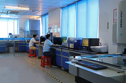
We have 55 QC, FQC, QA specialists who utilize 100 testing devices, advanced techniques like IMDS and PPAP. Our products are tested in physics lab strictly before shipment on every part number. And report will be included in carton. All of our pcbs are RoHs/Reach/CE compliant.


Staffs in Quality department get traning once per week to be skilled and professional.

Major test items:
outgoing insepction test micro section test solderability test temperature test thermal stress test electric test Full Inspection

FAQ

How about the shipment?

1. FedEx/DHL/UPS/TNT for samples, Door-to-Door;

2. By Air or by Sea for batch goods, for FCL; Airport/ Port receiving;
3. Delivery Time: 3-10 days for samples; 8-15 days for batch goods.

Shipment.jpg

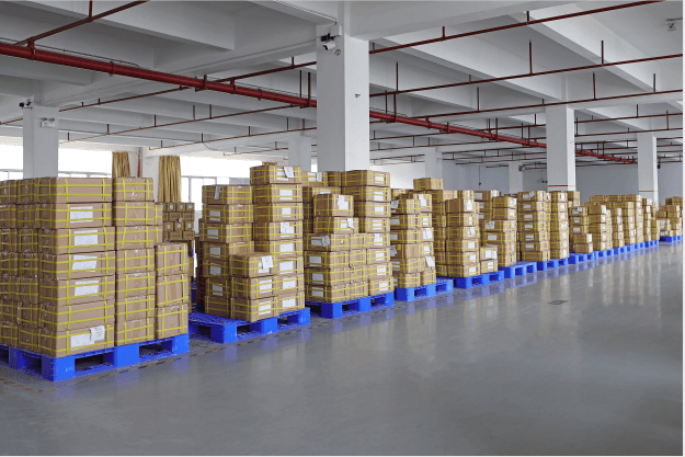
What‘s your package like?

1. Solid

2. Professional

3. No broken during the shipment

package victory pcb.png

Need it quick? That is our speciality!

Please call us on +86136 6225 0684, or mail us at sales@victorypcb.com

Case Reference

What is High-density multilayer PCB? HDI PCB Manufacturing Process

What is High-density multilayer PCB? HDI PCB Manufacturing Process

2021-09-09

If a PCB includes three or more layers or sheets of copper foil that are isolated from each other coating) and linked together to form a single component, it is called a high-density multilayer PCB. It must have at least three layers of conductive material buried in the material's center.

×

Contact Us

×

Inquire

*Name
*Email
Company Name
Tel
*Message

By continuing to use the site you agree to our privacy policy Terms and Conditions.

Recruit global agents and distributors Join us

I agree