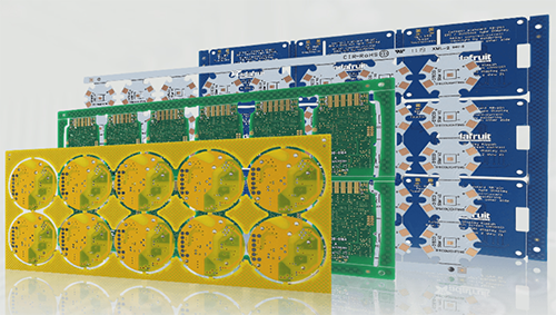
Many printed circuit board manufacturers are using heavy copper in their prototype productions. If you plan on doing the same, here are things to consider when using heavy copper in your PCB design.
Heavy Copper Considerations
On outer layers, there are two additional considerations for heavy copper. First and simplest is soldermask – when using liquid soldermask, multiple coats are required to adequately protect heavy copper traces. This problem is mitigated by 3D printed soldermask, but that technology is not available at every facility or in every color.
Second, surface mount pads can be compromised by heavy copper. Your Gerber file specifies the trace width at the base of the trace, but SMT happens on the top of the trace. With heavy copper, the top of the SMT pad may be several mils thinner than designed, leading to more difficult placement and potentially a weaker solder joint.

Cross-Sectional Area of Traces and Vias
One of the most important calculations in high current applications is the cross-sectional area of a trace. IPC 2152 shows (conservative) cross-sectional areas needed for particular amperages, but designers are left alone to calculate the area of a trapezoidal trace. Sure, the area of a trapezoid is h*(b1+b2)/2, h is obviously copper weight (in mils!) and b1 is obviously the trace width, but what is b2? Your PCB manufacturer’s sales and planning departments will know how much smaller the top of the trace is than the bottom, so be sure to ask them. Note that the difference varies from manufacturer to manufacturer.
Cross-sectional area of a via comes from knowing how much plating is in the via. With Class 2 plating, the via wall is 20 microns (0.0008”) thick. With Class 3 plating, the via wall is 25 microns (0.0010”) thick. Use these thicknesses and the diameter of your via to calculate the cross sectional area of a via, keeping in mind that the cross section makes an annulus. Note that Class 3 plating is commonly requested on Class 2 boards. Hole wall plating thicker than 25 microns is not difficult in low volumes, but is not recommended for a production part. Duplicating vias is usually a better solution than overplating. Using a conductive via fill helps only marginally. Via fill material is an epoxy, meaning that the current carrying capacity is not as high as pure silver or copper.
The Etching Process Has Improved
Heavy copper PCBs were once structured through a complex etching process. This process left uneven traces and inaccurate undercutting. Nowadays, when heavy copper is used in prototype productions, the etching process is more specialized and sound. Through technological advances, heavy copper features can now be formed by combining high-speed plating and differential etching. This process produces easy undercutting and even sidewalls.

Heat Rise and Current Flow Are Analogous
Heavy copper PCBs are capable of carrying current. However, how much current will vary depending on the thickness and width of the copper and the highest temperature rise the PCB can withstand. To determine the maximum current a trace can carry safely, you need to figure out the associated heat rise with the applied current.
The Benefits to Your Prototype Productions Are Numerous
When you use heavy copper for your PCB you get increased endurance to thermal strains and increased mechanical strength at the connector sites. In addition, when you use heavy copper you avoid circuit failure at high temperature, and the copper plated vias are able to carry higher current throughout the board to move heat to an external heatsink.

About Victory
Victory is a professional PCB manufacturer which established in 2005. Adhere to be a specialized manufacturer for multiply species, small to medium series, and quick turn production, we insist to provide 3H(high quality, high precision and high density) PCBs for our customers.
If you have any questions, please do not hesitate to contact us!