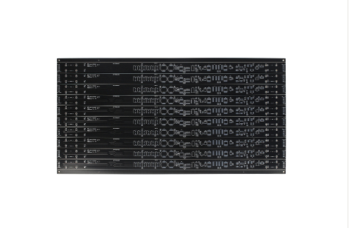
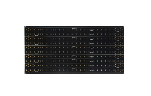
The main purpose of thickening copper plating is to ensure that there is a thick enough copper plating layer in the hole to ensure that the resistance value is within the range of the process requirements.
As a plug-in part, it is to fix the position and ensure the connection strength; as a surface-encapsulated device, some holes are only used as through holes, which play the role of conduction on both sides.
Copper plating process
In the process of thickening copper plating, the process parameters must be regularly monitored, which often causes unnecessary losses due to subjective and objective reasons. To do a good job in thickening copper plating process, you must do the following aspects:
1. Add a certain value based on the area value calculated by the computer and the empirical constant accumulated in actual production.

2. According to the calculated current value, in order to ensure the integrity of the coating in the hole, it is necessary to add a certain value to the original current value, that is, the impulse current, and then return to the original value in a short time.
3. When PCB electroplating reaches 5 minutes, take out the substrate and observe whether the copper layer on the surface and the inner wall of the hole is intact. It is better that all the holes have a metallic luster.
4. A certain distance must be maintained between the substrate and the substrate.
5. When the thick copper plating reaches the required electroplating time, a certain amount of current must be maintained during the removal of the substrate to ensure that the surface of the substrate and the hole will not be blackened or darkened.
Precautions:
1. Check the process documents, read the process requirements and be familiar with the blueprint of substrate machining.
2. Check the surface of the substrate for scratches, indentations, exposed copper parts, etc.
3. According to the mechanical processing floppy disk, carry out trial processing, carry out the first part pre-inspection, and then process all the workpieces after meeting the technological requirements.

4. Prepare the measuring tools and other tools used to monitor the geometric dimensions of the substrate.
5. According to the nature of the raw material of the processed substrate, select the appropriate milling tool.
Quality control
1. Strictly implement the first article inspection system to ensure that the product size meets the design requirements.
2. According to the raw materials of the PCB, the milling process parameters are reasonably selected.
3. When fixing the PCB position, carefully clamp it so as not to damage the solder layer and solder mask on the surface of the circuit board.
4. To ensure the consistency of the substrate dimensions, the position accuracy must be strictly controlled.
5. When disassembling and assembling, pay special attention to the padding of the barrier layer of the substrate to avoid damage to the coating layer on the PCB surface.
By continuing to use the site you agree to our privacy policy Terms and Conditions.
Recruit global agents and distributors Join us