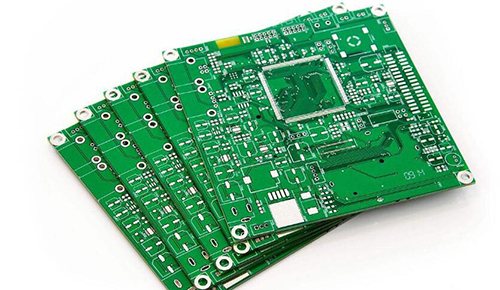
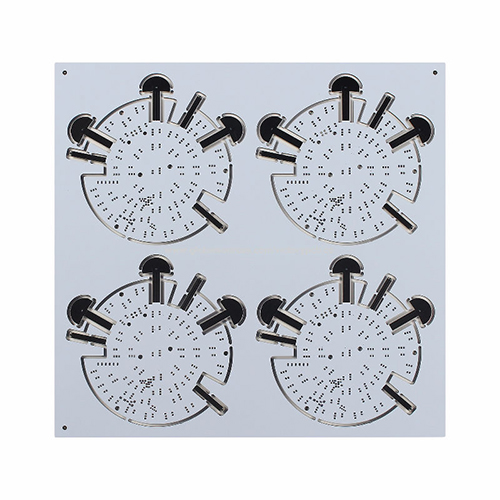
Double-sided PCB board is a very important PCB board in the circuit board. There are double-sided circuit board metal base PCB board, Hi-Tg heavy copper foil circuit board, flat and winding double-sided circuit board, and high-frequency circuit board on the market. PCB, hybrid dielectric base high frequency double-sided circuit board, etc., it is suitable for a wide range of high-tech industries.
There are wiring on both sides of the double-sided PCB board. However, to use wires on both sides, there must be a proper circuit connection between the two sides. The bridges between such circuits are called vias. A via is a small hole filled or coated with metal on the PCB, which can be connected with the wires on both sides.
A double-sided board is a printed circuit board with copper coated on both sides of the Top and Bottom. It is the most common and general-purpose circuit board. There are conductive patterns on both sides of the insulating substrate. The electrical connection on both sides is mainly through vias or soldering. Disk to connect. Because both sides can be routed, it greatly reduces the difficulty of wiring, so it is widely used.

Because the area of the double-sided board is twice as large as that of the single-sided board, the double-sided board solves the difficulty of interleaving wiring in the single-sided board (it can be connected to the other side through the hole), and it is more suitable for more complicated circuits than the single-sided board.
The production method of double-sided PCB board is generally made by the inner layer pattern first, and then the single-sided or double-sided substrate is made by printing and etching, and placed in the designated layer, and then heated, pressurized and bonded. As for the subsequent Drilling is the same as the plated through-hole method of double-sided board. These basic production methods have not changed much from the construction methods dating back to the 1960s, but with the materials and process technology (such as: pressure bonding technology, the solution of slag generated when drilling holes, the improvement of the film) have become more mature, and the attached The characteristics of pre-multilayer boards are more diverse.
The production of double-sided panels is more complicated than single-sided panels.
The main reasons are as follows:
(1) The top and bottom layers of the copper-clad board must be wired.
(2) The wires on the top and bottom layers should be connected with metallized vias.
Advantages:
1. They make it relatively easy to add conductive paths on the board, which means you will have a PCB that better suits your needs.

2. Since both sides of it are conductive, a large number of ICs and components can be assembled at any time.
3. There is an extra layer, so you can add more components as needed.
4. With more space and flexible design, it means that you are more likely to have a PCB that suits your requirements.
5. Double-sided PCB is an ideal choice for demanding applications and advanced electronic products.
6. If necessary, the size of the circuit board can be reduced, because double-sided can be used.
7. This type of PCB may save you money because you may only need to use one board.
Double-sided PCB can be used in many different applications and electronic products. In other words, they are ideal for a wide range of industries.
By continuing to use the site you agree to our privacy policy Terms and Conditions.
Recruit global agents and distributors Join us