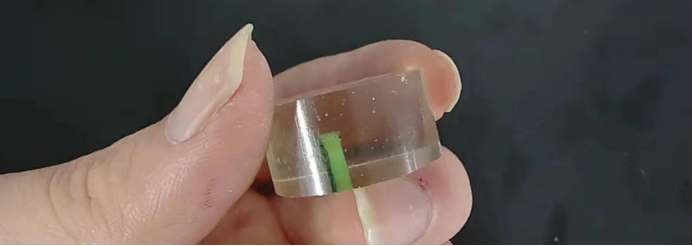
PCB Mircosection is mainly used to check the internal wiring thickness, layers of the PCB, the size of the through-hole and the quality observation of the through-hole. It is also used to check the internal cavity of the PCBA solder joint, the interface bonding condition and the wetting quality evaluation. The quality of the PCB, the occurrence and solution of problems and the evaluation of process improvement which need mircosection as the basis for objective examination, research and judgment. PCB Mircosection is one of the important analytical methods in PCB industry, which is often used for quality determination or quality abnormal analysis.
Cutting along the direction perpendicular of the PCB surface to observe the profile condition, which is usually used to observe the quality of the hole after copper plating, the lamination structure and the internal bonding surface condition. Vertical section is the most commonly used method in mircosection analysis.
It is used to grind down layers along the overlapping direction of the PCB to observe the condition of each layer.It is usually used to assist the analysis and determination of abnormal quality of vertical section, such as inside short or abnormal inside open.
In addition, there are also cut holes and oblique sections.
Sample taking: Taking samples from any position on the PCB with a special saw or cutting off the useless board with a cutting machine to get samples. Note that the latter can not be too close to the hole edge in order to prevent the through hole by pulling deformation.

2. Resin Encapsulation: The purpose is to clamp the sample mircosection to reduce deformation, the appropriate resin will be used to fill the through hole and seal the sample.
3. Grinding: The cutting force of sandpaper is used on the high-speed rotary table to grind the sample to the section in the center of the through hole, that is the plane where the center of the circle is located, so as to observe the section of the hole wall correctly. As for a small amount of simple sample cutting, as long as the sample in hand on the general sandpaper to grind back and forth.
4. Polishing: Seeing the detail of the mircosection must be carefully polished to eliminate the scratches of the sandpaper. Note that the direction of sample cutting should be changed frequently during polishing to produce a more uniform effect until the sand marks completely disappear.
5. Microetching: After washing and wiping the polishing surface, microetching can be carried out to distinguish the layers of metal and its crystallization state.
6. Photography: Assuming that the real effect of a good polished surface is 100%, the upside down image seen through the microscope can only be seen about 90~95% according to the performance of the machine.
After the mircosection is made, the mircosection analysis and interpretation are followed. To find out the cause of the adverse occurrence and make corresponding improvement measures, in order to improve the yield and reduce the loss.

Victory PCB can provide the mircosection when we finish the production and also receive nice feedback from our customer, welcome to contact us and looking forward to our cooperation.
By continuing to use the site you agree to our privacy policy Terms and Conditions.
Recruit global agents and distributors Join us