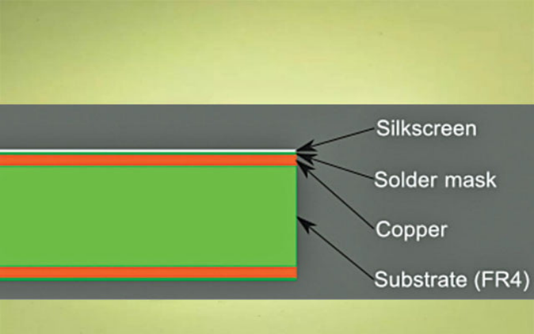
There are various types of substrates. Let's take a look at the differences and features of each.
Rigid substrates are substrates with patterns formed on a hard substrate. In other words, it cannot be bent. In general, when we say printed circuit board, this rigid circuit board is applicable. Rigid substrates cannot be bent, but are more durable and cheaper than flexible substrates, and are currently the mainstream.
A flexible substrate is a substrate on which a pattern is formed on a soft resin. Although it can be bent, it is expensive and less durable than a rigid board. It is mainly used when there is little space to embed the board and the board must be folded for mounting, or for moving parts.
A single-sided board is a printed circuit board in which patterns are placed on only one side of the board. Although it is the oldest and most basic printed circuit board, it is not suitable for complex electronic circuits. In addition, amateurs who like to assemble electronic circuits often use it.
A double-sided board is a printed circuit board that has patterns on both sides. Historically, it was the substrate that appeared after single-sided substrates, and it can handle somewhat complicated electronic circuits.
In addition, it is necessary to install a hole called a through hole as an electrical wiring that connects both sides. Through-holes connect one side of a double-sided board by making a hole in the board and pouring solder into the hole. This technology is essential for double-sided boards and multilayer boards.
Multi-layer boards are made by preparing multiple double-sided boards and compressing and bonding the multiple boards to create a board, which is currently the mainstream. Multi-layer boards are generally used for complex electronic circuits.
In the case of multi-layer boards, the pattern is etched for each layer and then layered later to manufacture, so it is essential that there is no misalignment when layered. In other words, the precision of overlay is required, so advanced technology is required for manufacturing.
There is also a classification based on the base material of the board. A baked board uses paper mixed with phenolic resin as the base of the board. Although the price is cheap, the high frequency characteristics are poor and the mechanical strength is also low. It seems that it is often used in low-priced electronic devices.
Paper-epoxy substrates are based on paper mixed with epoxy resin. A long time ago, this was the norm. The price is reasonable, and the high-frequency characteristics are better than the baked substrate, but glass epoxy is the mainstream nowadays, so it is not used much.
Glass-epoxy substrates are a mixture of glass fiber and epoxy resin, and are currently the mainstream. The price has come down enough from the past, and the high frequency characteristics are better than paper epoxy resin.
Alumina substrates are ceramic-based substrates, and are excellent in high-frequency characteristics and heat dissipation. Although it has the disadvantage of being expensive, it is mainly used in high-frequency, high-power circuits, taking advantage of these characteristics.
In addition, there are Teflon substrates that use fluorine resin as the base of the substrate.
The usual patterning method is called the subtractive method. This is done by preparing a printed circuit board with copper foil on the entire surface of the board and etching the unnecessary parts to form a pattern. There is also a special method called the additive method, in which the necessary parts are plated to form a pattern.
The rough printed circuit board creation process is as follows.
1. CUT MATERIAL: Cuts the raw material substrate to a pre-determined size. If the substrate size is small, multiple substrates will be processed at once, so in order to make it easier to cut after completion, small holes are drilled in a row or slits are opened.
2. Create Photomask: Create a photomask. For multi-layer boards, build layer by layer. In recent years, computers are used to design patterns, so it's not as difficult as it used to be.
3. Cleaning before material etching: Clean the surface of the substrate that will be the material. This removes excess dirt and makes the resist ride better.
Multi-layer boards, including 4-layer boards, are used to accommodate complex circuit formations and high-density component mounting.
Multi-layer boards such as 4-layer boards can accommodate circuit wiring that cannot be accommodated on single-sided or double-sided boards, making it possible to reduce the size, weight, and functionality of electronic devices.

In addition, multi-layer boards such as 4-layer boards are often used for what is generally called control boards, and are used for communication equipment such as personal computers that require excellent performance and high reliability.
Various devices are used in the etching process for forming circuit patterns.
· An auto-cut laminator that cuts dry film to a size suitable for the substrate and attaches it.
· An exposure device that exposes dry film by irradiating it with ultraviolet rays.
· Dry film developing machine that removes unnecessary dry film
· Etching equipment that dissolves unnecessary copper in the etching process to form circuit patterns

The characteristic impedance of the differential wiring increases at the portion crossing the slit. In the previous study, we found that the stronger the coupling in the differential wiring, the smaller the increase in the differential impedance at the slit-spanning portion, and that the transmission loss of the entire differential wiring with the slit-spanning can be estimated from this increase in differential impedance.
In the printed circuit board manufacturing process, processing machines are used to cut and drill the circuit board.
· A multi-cut former that neatly trims the end face after lamination press
· NC drill machine for drilling through holes
· NC router machine for processing the outer shape and mounting holes of the board
· V-cut machine for V-cut processing
The following equipment is used in the process of solder resist and silk printing, which is performed on the circuit board after forming the circuit pattern.
· A coater that applies and scatters solder resist on ink
· Exposure equipment for exposing solder resist
· A developer that removes unnecessary solder resist
· Inkjet printers and screen printers that print characters on substrates
The following inspection equipment is used in the inspection process to check and guarantee the quality of manufactured printed circuit boards.
· Flying checkers and dedicated checker devices that conduct continuity tests by contacting pins called probes with circuit patterns
· Hole checker to check if there are any abnormalities in through holes
· An automatic appearance inspection machine that checks for scratches and dirt on the surface and appearance of the board.
I introduced that the manufacturing method of printed circuit boards can be broadly divided into the subtractive method and the additive method. However, since the subtractive method can be further subdivided, there are many options for construction methods.
Since the optimum construction method changes depending on the pitch of the circuit pattern and the number of lots to be manufactured, it can be said that it is necessary to select the construction method after considering the specifications of the substrate that you want to manufacture in-house and the scale of your business.
Printed circuit boards are important components that determine whether electronic devices operate normally, and require a high level of quality. For this reason, many processes have already been automated using manufacturing equipment, and it is common to combine the manufacturing equipment responsible for each process into a production line.
However, work such as setting to manufacturing equipment, transportation, and visual inspection is done manually, and there are many companies whose work efficiency remains low.
In a multi-layer structure such as a four-layer board, heat transfer tends to be uneven and uneven. Therefore, when mounting a multilayer board through a reflow oven or flow bath, it is important to determine the temperature setting.
In addition, multi-layer boards require high-precision mounting equipment because the components are miniaturized and densely packed, and when soldering is corrected, more technology is required compared to single-sided boards. There will be
We are a company that specializes in surface mounting of printed circuit boards, flow soldering of hand-inserted parts, and unit assembly. We have extensive experience in multi-layer boards, including 4-layer boards.
In addition, we specialize in VA/VE proposals that maintain the functionality of the board drawn by the board designer and make changes to prevent defects and cost increases during mass production. We also have many achievements as an OEM manufacturer of control equipment.
· I want to reduce the production cost of the board.
· I want to make one at the prototype stage
· I want to know about OEM products
In recent years, GHz-class high-speed differential signals such as PCI Express and serial ATA have come into general use. The transmission path for differential signals on a printed circuit board is often a pair of +/- coupled lines, and the solid plane is often used as a reference plane.
It is ideal for this solid plane to be continuous from the standpoint of signal quality and EMC, but in reality, as the types of power supplies required for board operation increase, slits occur in the solid plane, and differential wiring intersects them. I have something to do.
However, the amount of increase in transmission loss is not large enough to directly cause malfunction of electronic equipment, and malfunction due to noise is more apprehensive.
In this article, we focus on the generation of noise caused by the crossing of slits in differential wiring, and report the results of actual measurements of magnetic field strength in the vicinity of a solid plane with slits.
Please contact us as we have 25 years of experience in mounting printed circuit boards and provide high-precision, high-quality products and technical know-how.
By continuing to use the site you agree to our privacy policy Terms and Conditions.
Recruit global agents and distributors Join us