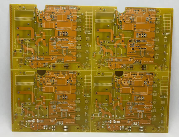
Just like the name suggests, stackup refers to the collection of copper and insulator layers that create a PCB before coming up with the final design of the board. There is a need for compacted electronic products, and that is why PCB layer stackup is pivotal in the electronics world. For electronic products to have that compacted design, designers see the need of putting up PCBs that contain multiple layers and a 3-dimensional outlook on the design. The multiple layers help with the following: increasing the capability of the board to distribute energy, supporting signals with high speed, eradicating electromagnetic interference, and minimizing cross-interference.

The final design of your board is essential. The design you come up with will determine the performance of the final product. For you to have a quality PCB stackup design, here are valuable tips you should put into consideration:
The first tip is for you to ascertain the number of layers. You should be aware of the quantity of layers that you need for the PCB stackup. This requires for you to put the following into consideration: power, signal, and ground layers. You can also consider planes. For the signal, you can consider either high or low speed. Electrical experts advice that you should not blend signal types on interior layers. For you have a precise layer count, you can make use of pin density. This is applicable for most boards.
Secondly, ascertain the layer arrangement. Once you have known the number of layers you need, the next thing is to ascertain how the arrangement will be or how the stackup will be. The rules to follow in this stage include:
1.Position signal layers close to inner power layers for the sake of tight coupling
2.There should be minimal space between power and ground layers
3.Make sure that 2 signal layers are not adjoining to each other
4. Ensure that the stackup has a symmetrical arrangement
Thirdly, decide on the materials of the layers. An essential factor to put into consideration for your PCB stackup is the thickness of every signal layer. A good tip for you to use when selecting the materials is the thermal, electrical, and mechanical properties of the materials. They should help you make the right decision concerning the materials to use.
Lastly, get to know the PCB routing and vias. For your PCB stackup design to be complete, you have to determine and route the traces. This process includes the following: ascertaining copper weights, the place to position vias and the kind of vias to apply.

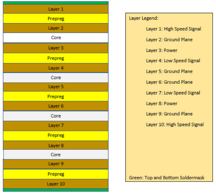
Above is an example of a PCB stackup design. It is possible to various stackup designs depending on the way a designer chooses to implement the above-mentioned tips.
By continuing to use the site you agree to our privacy policy Terms and Conditions.
Recruit global agents and distributors Join us