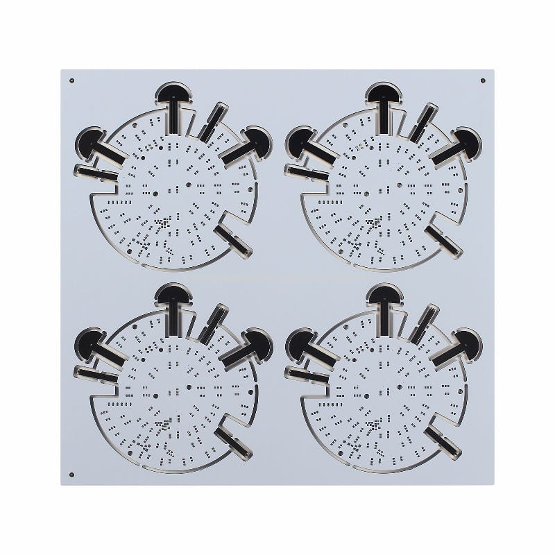
PCBs in the early stages were made with components present only on one side. However, today we have double-sided PCB, a more popular option because of its better applications and benefits.
As the name says, a double-sided PCB has circuit traces on both sides, connecting those layers at multiple points. So, the components and ICs soldered on both sides can communicate with each other to provide the right functionality required by the PCB.
These PCBs have several benefits, including the following.
A PCB with circuit traces on both sides saves space that another PCB would take. However, it adds more value because PCBs can be tighter, and the length of circuit traces between components can be reduced. It allows PCBs to provide much better performance because of their high density. Apart from high performance, these circuits are more efficient in terms of power consumption.

Designers find it easier to work on double-sided PCBs because of the 2 layers of circuit traces. Grounding components gets easier that would be very complex otherwise. Apart from flexibility, these PCBs are more reliable because double-sided designs make it possible to connect layers without any wires or pins instead of connecting multiple boards.
So, more than half of the work is done with efficient circuit designing for these PCBS. It also improves reliability because there are fewer physical joints and more circuit traces.
An amazing benefit of these PCBs is that they are not as complex as they sound. Although the designing process takes some calculations and expertise to be error-free, the complexity of these PCBs remains light to moderate.
These are not as simple as single-sided PCBs, but these are not the most complex PCBs one can work on. It enables these to be used in different electronics like smartphones, laptops, gadgets, etc.
Having multiple-layer PCBs for the same application you can do with double-sided PCBs will increase the cost. Double-sided PCBs come with much fewer costs for manufacturing and assembly because of having only 2 core layers to which components will be soldered.
Moving more components in less space also helps reduce the board's size, making them even cheaper and a better option for integrated devices. Having all components on one PCB also means you don't need communication components between different layers.
With such PCBs, the applications can become more compact. Smartphones today make the best examples because they become extremely compact and slim thanks to double-sided PCBs. Several other examples of electronics we use in our daily routine have become compact because of compact PCBs like TV, watches, computers, etc.
If you are designing a device, consider a double-sided PCB as the brain for this device. With advantages like high density and compactness, it may take your device leaps ahead.